The news
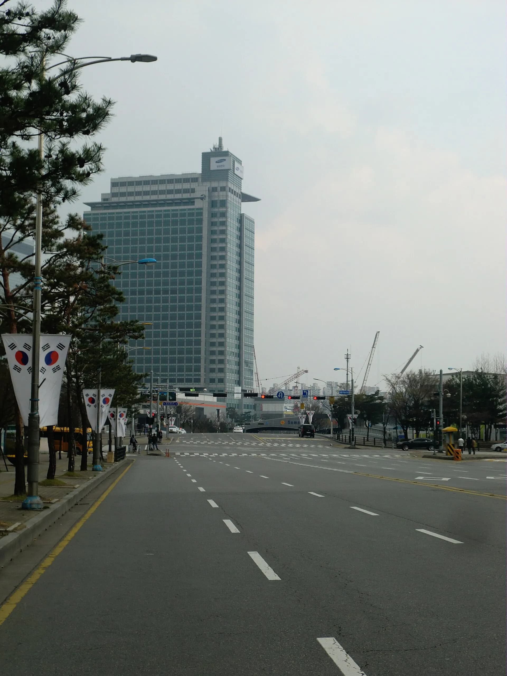
Samsung Electronics (005930.KS) and ASML (ASML) said on September 8, 2026, that they would expand their long-standing partnership, with a Samsung High NA EUV rollout planned for high-volume DRAM manufacturing by 2028, which the companies described as a first for the industry.
ASML's extreme ultraviolet (EUV) lithography machines print chip patterns onto silicon wafers. High NA models raise the numerical aperture of the optics, a measure of how finely they can focus light, from 0.33 to 0.55, TrendForce reported. The companies said High NA is expected to extend the DRAM scaling roadmap, because better resolution allows simpler processes and higher efficiency.
Samsung also said it will join an industry initiative to move to 12-inch photomasks, the patterned plates the machines project onto wafers. Chipmakers have used 6-inch masks for decades. According to the companies, larger masks are expected to raise fab productivity, lower chipmaking costs and remove stitching constraints, the need to expose big chips in pieces and join them. Samsung said it will work with partners on the mask technology and supporting infrastructure.
The initiative Samsung is joining was announced the same day by ASML and Taiwan Semiconductor Manufacturing Co. (TSM), according to TrendForce. The ASML and TSMC release set a goal of a 12-inch mask pilot line by 2031, with 12-inch High NA systems entering advanced-node production by 2033. TSMC said it intends to use High NA in high-volume manufacturing for advanced nodes starting in 2030, using current 6-inch masks at first.
Samsung Vice Chairman and CEO Young Hyun Jun said the AI era is raising the importance of technological innovation across the semiconductor value chain. ASML CEO Christophe Fouquet called Samsung "one of ASML's most important innovation partners" over many years. Neither company disclosed financial terms, the number of machines involved, or which DRAM generation or fab will use them first.
The numbers
- Samsung target for High NA EUV in DRAM volume production
- By 2028
- Numerical aperture, standard EUV vs High NA
- 0.33 vs 0.55
- Photomask size, current vs planned
- 6-inch vs 12-inch
- 12-inch mask pilot line target
- 2031
- 12-inch High NA systems in advanced-node production
- 2033
Why CEOs should care
For companies that buy servers and memory, this is a supply story on a 2028 clock. Samsung said in July that demand for server DRAM and high-bandwidth memory was expected to accelerate and keep the market undersupplied in the second half of 2026. High NA will not change that near term. What it may change is cost per bit later in the decade, if simpler patterning lets Samsung make more advanced DRAM per wafer. Procurement teams signing multi-year memory agreements should ask suppliers which process generations will reach volume in 2027 and 2028, and on what tools.
For CFOs and boards, the lesson is how long leading-edge roadmaps now run. The 12-inch mask transition is not expected to reach advanced-node production until 2033, and TSMC and Samsung are now lined up behind ASML's plan. Companies whose products depend on leading-edge memory or logic should treat ASML's timeline as a planning input and ask their chip suppliers how a delay in High NA or in the new mask format would affect delivery and pricing.
Investors should note what was not disclosed. Samsung gave no spending figure, no machine count and no named DRAM node. Until it does, the 2028 target is a plan, not a funded schedule anyone outside the company can check.
The bigger picture
The industry-first claim sits in a tight race. TrendForce, citing Yonhap, reported that Samsung brought in South Korea's first High NA system in March 2025. On September 3, 2025, TrendForce reported that SK hynix had installed an ASML TWINSCAN EXE:5200B, which it described as the first High NA model designed for volume production, at its M16 fab in Icheon. Samsung's claim is specifically about putting High NA into high-volume DRAM manufacturing.
The photomask initiative matters beyond memory. Getting TSMC and Samsung behind one 12-inch format gives mask makers and equipment suppliers a shared target, and the ASML and TSMC release said the change is expected to raise fab productivity, cut chipmaking costs and remove stitching constraints that High NA production faces with today's 6-inch masks.
What happened next
On September 9, 2026, TrendForce, citing the Korean outlet News1, reported that SK hynix plans to begin applying High NA EUV to DRAM mass production by 2028, and noted that Micron had not stated a timeline. On September 11, Digitimes, citing fnnews, reported the same SK hynix target and said the company was considering joining the 12-inch photomask initiative.
That makes 2028 a head-to-head deadline for Samsung and SK hynix. Watch for Samsung to name the DRAM generation and fab that will use High NA first, for any spending disclosure in its results, and for progress toward the 2031 mask pilot line.
What “Fact-checked” means
Fact-checking means testing a story’s facts against the evidence before it is published. This story went through at least two separate checks before this version was published.
- What we checked
- Its names, figures, dates, job titles, quotes and who said what were checked against the story’s sources, including its main source where it could be opened. The headline was checked for accuracy and overstatement.
- How
- A first check reviewed the whole story. If it passed, a second, skeptical check went back to the sources to look for mistakes in the most important facts. If a check flagged the story, it was edited to fix the problems found, and a separate re-check then reviewed the whole story again.
- Who
- The checks are made with our newsroom’s technology tools, as steps kept separate from the writing, under rules set by our editor, Hussein Mukhtar. A story the checks still flag is not published automatically; it is held for the editor, who decides whether it is fixed, published or dropped.
- Archive story
- It was written after the event. Its dates were checked against the date of the event, including the dates of any later developments it reports.
- If something is wrong
- “Fact-checked” does not mean error-free. If a material error is found after publication, we correct the story and add a note saying what changed. Report an error